The store will not work correctly when cookies are disabled.
JavaScript 似乎在您的浏览器中被禁用。
为了您在我们网站能获得最好的体验,建议在浏览器中打开Javascript。
MOSFETs
产品 描述 价格 库存 DC 数据手册 操作
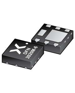
PSMN071-100NSEX
100NSE - N-channel 100 V, 82 mOhm standard level ASFET with enhanced SOA in DFN2020. Designed
for high power PoE, inrush management, eFuse and relay replacement
库存: 0
1+: ¥0.8662
500+: ¥0.7874
1000+: ¥0.7499
3000+: ¥0.7142
1+: ¥0.8662
500+: ¥0.7874
1000+: ¥0.7499
3000+: ¥0.7142
0
缺货
PSMN2R6-80YSFX
80YSF - NextPower 80 V, 2.4 mOhm, 231 A, N-channel MOSFET in LFPAK56E package
库存: 0
1+: ¥7.2416
500+: ¥6.5833
1000+: ¥6.2698
3000+: ¥5.9712
1+: ¥7.2416
500+: ¥6.5833
1000+: ¥6.2698
3000+: ¥5.9712
0
缺货
PSMN3R3-80YSFX
80YSF - NextPower 80 V, 3.1 mOhm, 160 A, N-channel MOSFET in LFPAK56 package
库存: 0
1+: ¥4.7419
500+: ¥4.3108
1000+: ¥4.1055
3000+: ¥3.9100
1+: ¥4.7419
500+: ¥4.3108
1000+: ¥4.1055
3000+: ¥3.9100
0
缺货
PSMNR90-40YSNX
40YSN - N-channel 40 V, 0.97 mOhm, 320 A, standard level MOSFET in LFPAK56 using
NextPower-S3 Schottky-Plus technology.
库存: 0
1+: ¥5.4674
500+: ¥4.9704
1000+: ¥4.7337
3000+: ¥4.5083
1+: ¥5.4674
500+: ¥4.9704
1000+: ¥4.7337
3000+: ¥4.5083
0
缺货
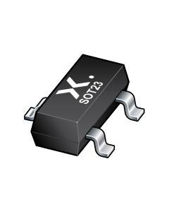
2N7002,215
channel Trench MOSFET
库存: 0
1+: ¥0.1129
500+: ¥0.1026
1000+: ¥0.0977
3000+: ¥0.0930
1+: ¥0.1129
500+: ¥0.1026
1000+: ¥0.0977
3000+: ¥0.0930
0
缺货
2N7002,235
channel Trench MOSFET
库存: 10000
1+: ¥0.1012
500+: ¥0.0920
1000+: ¥0.0878
3000+: ¥0.0836
1+: ¥0.1012
500+: ¥0.0920
1000+: ¥0.0878
3000+: ¥0.0836
10000
2N7002/HAMR
channel Trench MOSFET
库存: 3000
1+: ¥0.1061
500+: ¥0.0965
1000+: ¥0.0921
3000+: ¥0.0877
1+: ¥0.1061
500+: ¥0.0965
1000+: ¥0.0921
3000+: ¥0.0877
3000
2N7002BKV,115
channel Trench MOSFET
库存: 0
1+: ¥0.4959
500+: ¥0.4508
1000+: ¥0.4293
3000+: ¥0.4089
1+: ¥0.4959
500+: ¥0.4508
1000+: ¥0.4293
3000+: ¥0.4089
0
缺货
2N7002NXAKR
channel Trench MOSFET
库存: 0
1+: ¥0.0627
500+: ¥0.0570
1000+: ¥0.0544
3000+: ¥0.0518
1+: ¥0.0627
500+: ¥0.0570
1000+: ¥0.0544
3000+: ¥0.0518
0
缺货
2N7002NXBKR
channel Trench MOSFET
库存: 0
1+: ¥0.0751
500+: ¥0.0683
1000+: ¥0.0650
3000+: ¥0.0620
1+: ¥0.0751
500+: ¥0.0683
1000+: ¥0.0650
3000+: ¥0.0620
0
缺货
2N7002PV,115
channel Trench MOSFET
库存: 0
1+: ¥0.3799
500+: ¥0.3454
1000+: ¥0.3290
3000+: ¥0.3133
1+: ¥0.3799
500+: ¥0.3454
1000+: ¥0.3290
3000+: ¥0.3133
0
缺货
BSH103,215
30 V, N-channel Trench MOSFET
库存: 0
1+: ¥0.9314
500+: ¥0.8870
1000+: ¥0.8448
3000+: ¥0.8046
1+: ¥0.9314
500+: ¥0.8870
1000+: ¥0.8448
3000+: ¥0.8046
0
缺货
 PSMN071-100NSEXPSMN071PSMN071-100NSEX100NSE - N-channel 100 V, 82 mOhm standard level ASFET with enhanced SOA in DFN2020. Designed for high power PoE, inrush management, eFuse and relay replacement库存: 01+: ¥0.8662500+: ¥0.78741000+: ¥0.74993000+: ¥0.71421+: ¥0.8662500+: ¥0.78741000+: ¥0.74993000+: ¥0.71420
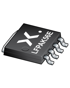 PSMN2R6-80YSFXPSMN2R6PSMN2R6-80YSFX80YSF - NextPower 80 V, 2.4 mOhm, 231 A, N-channel MOSFET in LFPAK56E package库存: 01+: ¥7.2416500+: ¥6.58331000+: ¥6.26983000+: ¥5.97121+: ¥7.2416500+: ¥6.58331000+: ¥6.26983000+: ¥5.97120
 PSMN3R3-80YSFXPSMN3R3PSMN3R3-80YSFX80YSF - NextPower 80 V, 3.1 mOhm, 160 A, N-channel MOSFET in LFPAK56 package库存: 01+: ¥4.7419500+: ¥4.31081000+: ¥4.10553000+: ¥3.91001+: ¥4.7419500+: ¥4.31081000+: ¥4.10553000+: ¥3.91000
 PSMNR90-40YSNXPSMNR90PSMNR90-40YSNX40YSN - N-channel 40 V, 0.97 mOhm, 320 A, standard level MOSFET in LFPAK56 using NextPower-S3 Schottky-Plus technology.库存: 01+: ¥5.4674500+: ¥4.97041000+: ¥4.73373000+: ¥4.50831+: ¥5.4674500+: ¥4.97041000+: ¥4.73373000+: ¥4.50830
 2N7002,2352N70021+: ¥0.1012500+: ¥0.09201000+: ¥0.08783000+: ¥0.083610000
 2N7002/HAMR2N70021+: ¥0.1061500+: ¥0.09651000+: ¥0.09213000+: ¥0.08773000
 BSH103,215BSH1031+: ¥0.9314500+: ¥0.88701000+: ¥0.84483000+: ¥0.80460