The store will not work correctly when cookies are disabled.
氮化镓场效应晶体管(GaN FET)
- 产品
- 描述
- 价格
- 库存
- DC
- 数据手册
- 操作
-
GAN041-650WSBQ
650WSB - 650 V, 35 mΩ Gallium Nitride (GaN) FET in a TO-247 package
库存: 0
1+: ¥57.7437
500+: ¥52.4943
1000+: ¥49.9946
3000+: ¥47.6139
1+: ¥57.7437
500+: ¥52.4943
1000+: ¥49.9946
3000+: ¥47.6139
0
-
GAN039-650NBBHP
650NBB - 650 V, 33 mOhm Gallium Nitride (GaN) FET in a CCPAK1212 package
库存: 0
1+: ¥62.0369
500+: ¥56.3972
1000+: ¥53.7116
3000+: ¥51.1539
1+: ¥62.0369
500+: ¥56.3972
1000+: ¥53.7116
3000+: ¥51.1539
0
-
GAN039-650NTBZ
650NTB - 650 V, 33 mOhm Gallium Nitride (GaN) FET in a CCPAK1212i package
库存: 0
1+: ¥58.9794
500+: ¥53.6177
1000+: ¥51.0644
3000+: ¥48.6328
1+: ¥58.9794
500+: ¥53.6177
1000+: ¥51.0644
3000+: ¥48.6328
0
-
GAN063-650WSAQ
650WSA - 650 V, 50 mΩ Gallium Nitride (GaN) FET
库存: 0
1+: ¥98.3146
500+: ¥89.3769
1000+: ¥85.1208
3000+: ¥81.0675
1+: ¥98.3146
500+: ¥89.3769
1000+: ¥85.1208
3000+: ¥81.0675
0
-
GAN080-650EBEZ
650EBE - 650 V, 80 mOhm Gallium Nitride (GaN) FET in a DFN 8 mm x 8 mm package
库存: 2452
1+: ¥28.1205
500+: ¥25.5641
1000+: ¥24.3468
3000+: ¥23.1874
1+: ¥28.1205
500+: ¥25.5641
1000+: ¥24.3468
3000+: ¥23.1874
2452
-
GAN140-650EBEZ
650EBE - 650 V, 140 mOhm Gallium Nitride (GaN) FET in a DFN 8 mm x 8 mm package
库存: 2465
1+: ¥19.2121
500+: ¥17.4656
1000+: ¥16.6339
3000+: ¥15.8418
1+: ¥19.2121
500+: ¥17.4656
1000+: ¥16.6339
3000+: ¥15.8418
2465
-
GAN140-650FBEZ
650FBE - 650 V, 140 mOhm Gallium Nitride (GaN) FET in a DFN 5 mm x 6 mm package
库存: 2472
1+: ¥17.9242
500+: ¥16.2947
1000+: ¥15.5188
3000+: ¥14.7798
1+: ¥17.9242
500+: ¥16.2947
1000+: ¥15.5188
3000+: ¥14.7798
2472
-
GAN190-650EBEZ
650EBE - 650 V, 190 mOhm Gallium Nitride (GaN) FET in a DFN 8 mm x 8 mm package
库存: 2481
1+: ¥12.2357
500+: ¥11.1233
1000+: ¥10.5936
3000+: ¥10.0892
1+: ¥12.2357
500+: ¥11.1233
1000+: ¥10.5936
3000+: ¥10.0892
2481
-
GAN190-650FBEZ
650FBE - 650 V, 190 mOhm Gallium Nitride (GaN) FET in a DFN 5 mm x 6 mm package
库存: 2487
1+: ¥11.4843
500+: ¥10.4403
1000+: ¥9.9432
3000+: ¥9.4697
1+: ¥11.4843
500+: ¥10.4403
1000+: ¥9.9432
3000+: ¥9.4697
2487
-
GAN3R2-100CBEAZ
100CBE - 100 V, 3.2 mOhm Gallium Nitride (GaN) FET in a 3.5 mm x 2.13 mm Wafer Level Chip-Scale
Package (WLCSP)
库存: 2970
1+: ¥14.2749
500+: ¥12.9772
1000+: ¥12.3592
3000+: ¥11.7707
1+: ¥14.2749
500+: ¥12.9772
1000+: ¥12.3592
3000+: ¥11.7707
2970
-
GAN7R0-150LBEZ
150LBE - 150 V, 7 mOhm Gallium Nitride (GaN) FET in a 2.2 mm x 3.2 mm x 0.774 mm Land Grid Array
(LGA) package
库存: 989
1+: ¥10.7330
500+: ¥9.7573
1000+: ¥9.2927
3000+: ¥8.8502
1+: ¥10.7330
500+: ¥9.7573
1000+: ¥9.2927
3000+: ¥8.8502
989
 GAN041-650WSBQGAN041GAN041-650WSBQ650WSB - 650 V, 35 mΩ Gallium Nitride (GaN) FET in a TO-247 package库存: 01+: ¥57.7437500+: ¥52.49431000+: ¥49.99463000+: ¥47.61391+: ¥57.7437500+: ¥52.49431000+: ¥49.99463000+: ¥47.61390
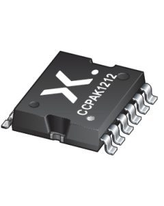 GAN039-650NBBHPGAN039GAN039-650NBBHP650NBB - 650 V, 33 mOhm Gallium Nitride (GaN) FET in a CCPAK1212 package库存: 01+: ¥62.0369500+: ¥56.39721000+: ¥53.71163000+: ¥51.15391+: ¥62.0369500+: ¥56.39721000+: ¥53.71163000+: ¥51.15390
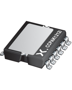 GAN039-650NTBZGAN039GAN039-650NTBZ650NTB - 650 V, 33 mOhm Gallium Nitride (GaN) FET in a CCPAK1212i package库存: 01+: ¥58.9794500+: ¥53.61771000+: ¥51.06443000+: ¥48.63281+: ¥58.9794500+: ¥53.61771000+: ¥51.06443000+: ¥48.63280
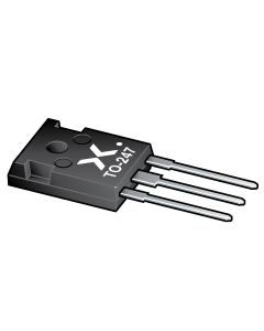 GAN063-650WSAQGAN063GAN063-650WSAQ650WSA - 650 V, 50 mΩ Gallium Nitride (GaN) FET库存: 01+: ¥98.3146500+: ¥89.37691000+: ¥85.12083000+: ¥81.06751+: ¥98.3146500+: ¥89.37691000+: ¥85.12083000+: ¥81.06750
 GAN080-650EBEZGAN080GAN080-650EBEZ650EBE - 650 V, 80 mOhm Gallium Nitride (GaN) FET in a DFN 8 mm x 8 mm package库存: 24521+: ¥28.1205500+: ¥25.56411000+: ¥24.34683000+: ¥23.18741+: ¥28.1205500+: ¥25.56411000+: ¥24.34683000+: ¥23.18742452
 GAN140-650EBEZGAN140GAN140-650EBEZ650EBE - 650 V, 140 mOhm Gallium Nitride (GaN) FET in a DFN 8 mm x 8 mm package库存: 24651+: ¥19.2121500+: ¥17.46561000+: ¥16.63393000+: ¥15.84181+: ¥19.2121500+: ¥17.46561000+: ¥16.63393000+: ¥15.84182465
 GAN140-650FBEZGAN140GAN140-650FBEZ650FBE - 650 V, 140 mOhm Gallium Nitride (GaN) FET in a DFN 5 mm x 6 mm package库存: 24721+: ¥17.9242500+: ¥16.29471000+: ¥15.51883000+: ¥14.77981+: ¥17.9242500+: ¥16.29471000+: ¥15.51883000+: ¥14.77982472
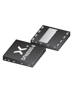 GAN190-650EBEZGAN190GAN190-650EBEZ650EBE - 650 V, 190 mOhm Gallium Nitride (GaN) FET in a DFN 8 mm x 8 mm package库存: 24811+: ¥12.2357500+: ¥11.12331000+: ¥10.59363000+: ¥10.08921+: ¥12.2357500+: ¥11.12331000+: ¥10.59363000+: ¥10.08922481
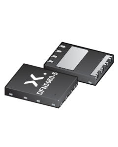 GAN190-650FBEZGAN190GAN190-650FBEZ650FBE - 650 V, 190 mOhm Gallium Nitride (GaN) FET in a DFN 5 mm x 6 mm package库存: 24871+: ¥11.4843500+: ¥10.44031000+: ¥9.94323000+: ¥9.46971+: ¥11.4843500+: ¥10.44031000+: ¥9.94323000+: ¥9.46972487
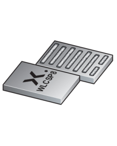 GAN3R2-100CBEAZGAN3R2GAN3R2-100CBEAZ100CBE - 100 V, 3.2 mOhm Gallium Nitride (GaN) FET in a 3.5 mm x 2.13 mm Wafer Level Chip-Scale Package (WLCSP)库存: 29701+: ¥14.2749500+: ¥12.97721000+: ¥12.35923000+: ¥11.77071+: ¥14.2749500+: ¥12.97721000+: ¥12.35923000+: ¥11.77072970
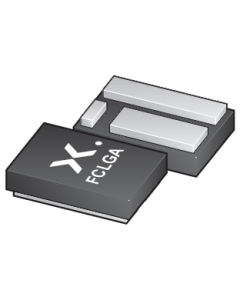 GAN7R0-150LBEZGAN7R0GAN7R0-150LBEZ150LBE - 150 V, 7 mOhm Gallium Nitride (GaN) FET in a 2.2 mm x 3.2 mm x 0.774 mm Land Grid Array (LGA) package库存: 9891+: ¥10.7330500+: ¥9.75731000+: ¥9.29273000+: ¥8.85021+: ¥10.7330500+: ¥9.75731000+: ¥9.29273000+: ¥8.8502989