The store will not work correctly when cookies are disabled.
折扣专区
- 产品
- 描述
- 价格
- 库存
- DC
- 数据手册
- 操作
-
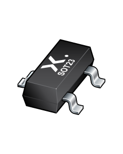
PLVA665A-QR
Q_SER - Low-voltage avalanche regulator diodes
库存: 3000
1+: ¥0.3306
500+: ¥0.3005
1000+: ¥0.2862
3000+: ¥0.1488
1+: ¥0.3306
500+: ¥0.3005
1000+: ¥0.2862
3000+: ¥0.1488
3000
-
BZT52-B6V2-QX
Q series - Voltage regulator diodes
库存: 3000
1+: ¥0.1148
500+: ¥0.1044
1000+: ¥0.0994
3000+: ¥0.0523
1+: ¥0.1148
500+: ¥0.1044
1000+: ¥0.0994
3000+: ¥0.0523
3000
-
1+: ¥3.0000
3000+: ¥0.0780
3000
-
BZT52H-A20-QX
Q series - Voltage regulator diodes
库存: 3000
1+: ¥0.9703
500+: ¥0.8821
1000+: ¥0.8401
3000+: ¥0.4361
1+: ¥0.9703
500+: ¥0.8821
1000+: ¥0.8401
3000+: ¥0.4361
3000
-
BZX84-A27-QR
Voltage regulator diodes
库存: 0
1+: ¥0.9703
500+: ¥0.8821
1000+: ¥0.8401
3000+: ¥0.4361
1+: ¥0.9703
500+: ¥0.8821
1000+: ¥0.8401
3000+: ¥0.4361
0
-
NPS4001GVH
5.5 V, 55 mOhm load switch with current limitation
库存: 3000
1+: ¥0.9660
500+: ¥0.8782
1000+: ¥0.8363
3000+: ¥0.4345
1+: ¥0.9660
500+: ¥0.8782
1000+: ¥0.8363
3000+: ¥0.4345
3000
-
1+: ¥3.0000
3000+: ¥0.1561
3000
-
1+: ¥3.0000
3000+: ¥0.0668
3000
-
1+: ¥3.0000
3000+: ¥0.1376
3000
-
1+: ¥3.0000
3000+: ¥0.0571
3000
-
1+: ¥3.0000
3000+: ¥0.0571
0
-
1+: ¥3.0000
3000+: ¥0.0571
3000

 PLVA665A-QRvp_PLVA6XXAPLVA665A-QRQ_SER - Low-voltage avalanche regulator diodes库存: 30001+: ¥0.3306500+: ¥0.30051000+: ¥0.28623000+: ¥0.14881+: ¥0.3306500+: ¥0.30051000+: ¥0.28623000+: ¥0.14883000
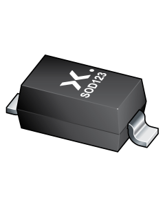 BZT52-B6V2-QXBZT52BZT52-B6V2-QXQ series - Voltage regulator diodes库存: 30001+: ¥0.1148500+: ¥0.10441000+: ¥0.09943000+: ¥0.05231+: ¥0.1148500+: ¥0.10441000+: ¥0.09943000+: ¥0.05233000
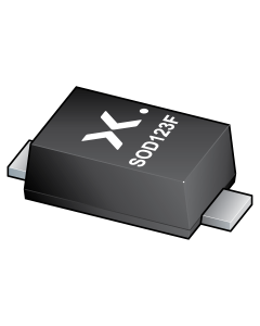 BZT52H-A20-QXBZT52HBZT52H-A20-QXQ series - Voltage regulator diodes库存: 30001+: ¥0.9703500+: ¥0.88211000+: ¥0.84013000+: ¥0.43611+: ¥0.9703500+: ¥0.88211000+: ¥0.84013000+: ¥0.43613000
 BZX84-A27-QRBZX84 series1+: ¥0.9703500+: ¥0.88211000+: ¥0.84013000+: ¥0.43610
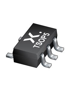 NPS4001GVHNPS4001NPS4001GVH5.5 V, 55 mOhm load switch with current limitation库存: 30001+: ¥0.9660500+: ¥0.87821000+: ¥0.83633000+: ¥0.43451+: ¥0.9660500+: ¥0.87821000+: ¥0.83633000+: ¥0.43453000