图像仅供参考
请参阅产品规格
-
商品编号:
AXP1T34GMX
-
简述:
Dual supply translating buffer
-
描述:
The AXP1T34 is a single bit, dual supply translating buffer. It features one input (A), an output (Y) and dual supply pins (VCCI and VCCO). Both VCCI and VCCO can be supplied at any voltage between 0.9 V and 5.5 V making the device suitable for translating between any voltage nodes specified (1.2 V, 1.5 V, 1.8 V, 2.5 V, 3.3 V and 5.0 V). No power supply sequencing is required and output glitches during power supply transitions are prevented using patented circuitry. As a result, glitches will not appear on the outputs for supply transitions during power-up/down between 20 mV/μs and 5.5 V/s
The input is referenced to VCCI and the output is referenced to VCCO. Schmitt-trigger action at the input makes the circuit tolerant of slower input rise and fall times.
This device ensures low static and dynamic power consumption across the entire supply range and is fully specified for partial power down applications using IOFF. The IOFF circuitry disables the output, preventing the potentially damaging backflow current through the device when it is powered down. In suspend mode when either VCCI or VCCO are at GND level the output is in the high-impedance OFF-state
- 数据手册:
特性
Wide supply voltage range:
VCCI: 0.9 V to 5.5 V
VCCO: 0.9 V to 5.5 V
Low input capacitance; CI = 1.5 pF (typical)
Low output capacitance; CO = 3.8 pF (typical)
Low dynamic power consumption; CPD = 0.4 pF at VCCI = 1.2 V (typical)
Low dynamic power consumption; CPD = 11 pF at VCCO = 5 V (typical)
Low static power consumption; ICCI = 0.1 µA (25 °C maximum)
Low static power consumption; ICCO = 1.0 µA (25 °C maximum)
High noise immunity
Complies with JEDEC standard:
JESD8-12 (1.1 V to 1.3 V; A input)
JESD8-11 (1.4 V to 1.6 V)
JESD8-7 (1.65 V to 1.95 V)
JESD8-5 (2.3 V to 2.7 V)
JESD8C (2.7 V to 3.6 V)
JESD12-6 (4.5 V to 5.5 V)
ESD protection:
HBM: ANSI/ESDA/JEDEC JS-001 class 2 exceeds 2000 V
CDM: ANSI/ESDA/JEDEC JS-002 class C3 exceeds 1000 V
Latch-up performance exceeds 100 mA per JESD78D Class II
Inputs accept voltages up to 5.5 V
Low noise overshoot and undershoot < 10% of VCCO
IOFF circuitry provides partial power-down mode operation
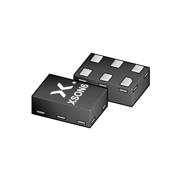
Multiple package options
Specified from −40 °C to +125 °C