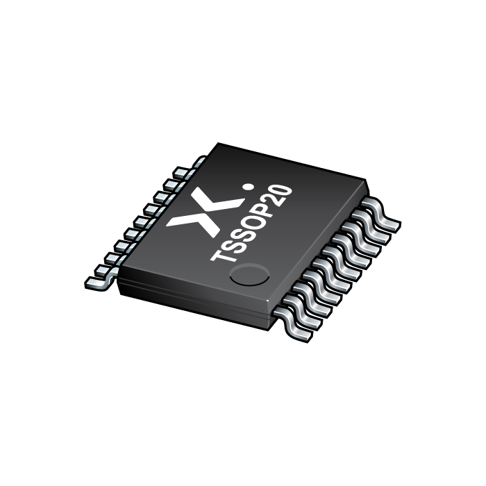
图像仅供参考
请参阅产品规格
-
商品编号:
74LVC8T595PWJ
-
简述:
Dual supply 8-bit serial-in/serial-out or parallel-out shift register; 3-state
-
描述:
The 74LVC8T595 is an 8-bit serial-in/serial or parallel-out shift register with a storage register and 3-state outputs. Both the shift and storage register have separate clocks. Data is shifted on the positive-going transitions of the SHCP input. The data in the shift register is transferred to the storage register on a positive-going transition of the STCP input. If both clocks are connected together, the shift register is always one clock pulse ahead of the storage register.
VCC(A) and VCC(B) can be supplied at any voltage between 1.1 V and 5.5 V making the device suitable for translating between any of the voltage nodes (1.2 V, 1.5 V, 1.8 V, 2.5 V, 3.3 V and 5.0 V). Pins MR, SHCP, STCP, OE, DS and Q7S are referenced to VCC(A) and pins Qn are referenced to VCC(B).
The device is fully specified for partial power-down applications using IOFF. The IOFF circuitry disables the output, preventing any damaging backflow current through the device when it is powered down. In suspend mode when VCC(A) is at GND level, the Qn outputs are in the high-impedance OFF-state.
- 数据手册:
特性
Wide supply voltage range:
VCC(A): 1.1 V to 5.5 V
VCC(B): 1.1 V to 5.5 V
High noise immunity
Suspend mode
Latch-up performance exceeds 100 mA per JESD 78 Class II
±24 mA output drive (VCC(A) = VCC(B) = 3.0 V)
Inputs accept voltages up to 5.5 V
IOFF circuitry provides partial Power-down mode operation
Complies with JEDEC standards:
JESD8-12A (1.1 V to 1.3 V)
JESD8-11A (1.4 V to 1.6 V)
JESD8-7 (1.65 V to 1.95 V)
JESD8-5 (2.3 V to 2.7 V)
JESD8C (3.0 V to 3.6 V)
JESD12-6 (4.5 V to 5.5 V)
ESD protection:
HBM: ANSI/ESDA/JEDEC JS-001 class 3A exceeds 4000 V
CDM: ANSI/ESDA/JEDEC JS-002 class C3 exceeds 1000 V
Specified from -40 °C to +85 °C and -40 °C to +125 °C