图像仅供参考
请参阅产品规格
-
商品编号:
74LVC4066PW-Q100J
-
简述:
Q100 - Quad bilateral switch
-
描述:
The 74LVC4066-Q100 is a high-speed Si-gate CMOS device.
The 74LVC4066-Q100 provides four single pole, single-throw analog switch functions. Each switch has two input/output terminals (nY and nZ) and an active HIGH enable input (nE). When nE is LOW, the analog switch is turned off.
Schmitt-trigger action at the enable inputs makes the circuit tolerant of slower input rise and fall times across the entire VCC range from 1.65 V to 5.5 V.
This product has been qualified to the Automotive Electronics Council (AEC) standard Q100 (Grade 1) and is suitable for use in automotive applications.
- 数据手册:
特性
Automotive product qualification in accordance with AEC-Q100 (Grade 1)
Specified from -40 °C to +85 °C and from -40 °C to +125 °C
Wide supply voltage range from 1.65 V to 5.5 V
Very low ON resistance:
7.5 Ω (typical) at VCC = 2.7 V
6.5 Ω (typical) at VCC = 3.3 V
6 Ω (typical) at VCC = 5 V
Switch current capability of 32 mA
High noise immunity
CMOS low-power consumption
Direct interface TTL-levels
Latch-up performance exceeds 250 mA
Enable inputs accept voltages up to 5 V
ESD protection:
HBM: ANSI/ESDA/JEDEC JS-001 class 2 exceeds 2000 V
CDM: ANSI/ESDA/JEDEC JS-002 class C3 exceeds 1000 V
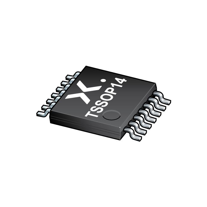
Multiple package options
DHVQFN package with Side-Wettable Flanks enabling Automatic Optical Inspection (AOI) of solder joints