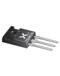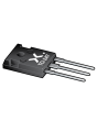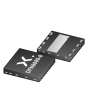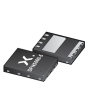
图像仅供参考
请参阅产品规格
-
商品编号:
74LVC1G99GT,115
-
简述:
Ultra-configurable multiple function gate; 3-state
-
描述:
The 74LVC1G99 provides a low voltage, ultra-configurable, multiple function gate with 3-state output. The device can be configured as one of several logic functions including, AND, OR, NAND, NOR, XOR, XNOR, inverter, buffer and MUX. No external components are required to configure the device as all inputs can be connected directly to VCC or GND. The 3-state output is controlled by the output enable input (OE). A HIGH level at OE causes the output (Y) to assume a high-impedance OFF-state. When OE is LOW, the output state is determined by the signals applied to the Schmitt trigger inputs (A, B, C and D).
Due to the use of Schmitt trigger inputs the device is tolerant of slowly changing input signals, transforming them into sharply defined, jitter free output signals. By eliminating leakage current paths to VCC and GND, the inputs and disabled output are also over-voltage tolerant, making the device suitable for mixed-voltage applications.
This device is fully specified for partial power-down applications using IOFF. The IOFF circuitry disables the output, preventing the damaging backflow current through the device when it is powered down.
The 74LVC1G99 is fully specified over the supply range from 1.65 V to 5.5 V.
- 数据手册:
特性
Wide supply voltage range from 1.65 V to 5.5 V
5 V tolerant inputs for interfacing with 5 V logic
High noise immunity
±24 mA output drive (VCC = 3.0 V)
CMOS low power consumption
Latch-up performance exceeds 250 mA
Direct interface with TTL levels
Inputs accept voltages up to 5 V
Complies with JEDEC standard:
JESD8-7 (1.65 V to 1.95 V)
JESD8-5 (2.3 V to 2.7 V)
JESD8-B/JESD36 (2.7 V to 3.6 V)
ESD protection:
HBM: ANSI/ESDA/JEDEC JS-001 class 2 exceeds 2000 V
CDM: ANSI/ESDA/JEDEC JS-002 class C3 exceeds 1000 V
Multiple package options
Specified from -40 °C to +85 °C and -40 °C to +125 °C.