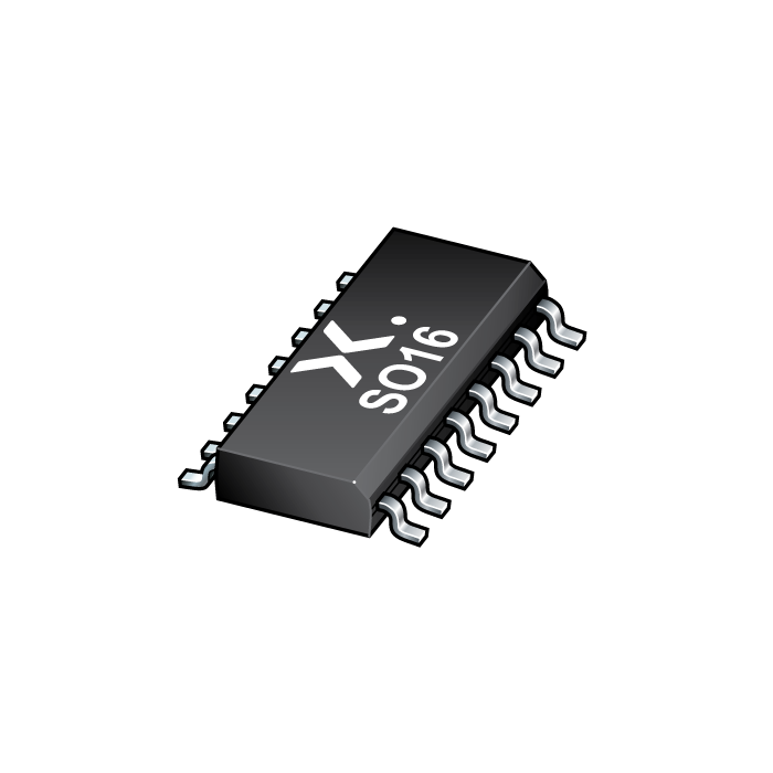
图像仅供参考
请参阅产品规格
-
商品编号:
74HCT259D-Q100,118
-
简述:
Q100; 74HCT259-Q100 - 8-bit addressable latch
-
描述:
The 74HC259-Q100; 74HCT259-Q100 is an 8-bit addressable latch. The device features four modes of operation. In the addressable latch mode, data on the D input is written into the latch addressed by the inputs A0 to A3. The addressed latch will follow the data input, non-addressed latches will retain their previous states. In memory mode, all latches retain their previous states and are unaffected by the data or address inputs. In the 3-to-8 decoding or demultiplexing mode, the addressed output follows the D input and all other outputs are LOW. In the reset mode, all outputs are forced LOW and unaffected by the data or address inputs. Inputs include clamp diodes. This enables the use of current limiting resistors to interface inputs to voltages in excess of VCC.
This product has been qualified to the Automotive Electronics Council (AEC) standard Q100 (Grade 1) and is suitable for use in automotive applications.
- 数据手册:
特性
Automotive product qualification in accordance with AEC-Q100 (Grade 1)
Specified from -40 °C to +85 °C and from -40 °C to +125 °C
Wide supply voltage range from 2.0 V to 6.0 V
Latch-up performance exceeds 100 mA per JESD 78 Class II Level B
Complies with JEDEC standards:
- JESD8C (2.7 V to 3.6 V)
- JESD7A (2.0 V to 6.0 V)
Combined demultiplexer and 8-bit latch
Serial-to-parallel capability
Output from each storage bit available
Random (addressable) data entry
Easily expandable
Common reset input
Useful as a 3-to-8 active HIGH decoder
Input levels:
For 74HC259-Q100: CMOS level
For 74HCT259-Q100: TTL level
ESD protection:
HBM: ANSI/ESDA/Jedec JS-001 Class 2 exceeds 2000 V
Multiple package options
DHVQFN package with Side-Wettable Flanks enabling Automatic Optical Inspection (AOI) of solder joints