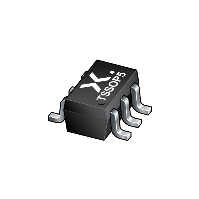
图像仅供参考
请参阅产品规格
-
商品编号:
74AUP1T08GW-Q100H
-
简述:
Q100 - Low-power 2-input AND gate with voltage-level translator
-
描述:
The 74AUP1T08-Q100 provides the single 2-input AND function. This device ensures a very low static and dynamic power consumption across the entire VCC range from 2.3 V to 3.6 V.
The 74AUP1T08-Q100 is designed for logic-level translation applications with input switching levels that accept 1.8 V low-voltage CMOS signals, while operating from either a single 2.5 V or 3.3 V supply voltage.
The wide supply voltage range ensures normal operation as battery voltage drops from 3.6 V to 2.3 V.
This device is fully specified for partial power-down applications using IOFF. The IOFF circuitry disables the output, preventing the damaging backflow current through the device when it is powered down.
Schmitt trigger inputs make the circuit tolerant to slower input rise and fall times across the entire VCC range.
This product has been qualified to the Automotive Electronics Council (AEC) standard Q100 (Grade 1) and is suitable for use in automotive applications.
- 数据手册:
特性
Automotive product qualification in accordance with AEC-Q100 (Grade 1)
Specified from -40 °C to +85 °C and from -40 °C to +125 °C
Wide supply voltage range from 2.3 V to 3.6 V
High noise immunity
Low static power consumption; ICC = 1.5 μA (maximum)
Latch-up performance exceeds 100 mA per JESD 78 Class II
Inputs accept voltages up to 3.6 V
Low noise overshoot and undershoot < 10 % of VCC
IOFF circuitry provides partial power-down mode operation
ESD protection:
HBM: ANSI/ESDA/JEDEC JS-001 class 3A exceeds 5000 V
CDM: ANSI/ESDA/JEDEC JS-002 class C3 exceeds 1000 V


