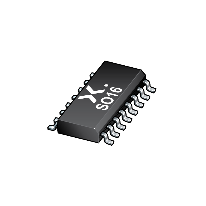
图像仅供参考
请参阅产品规格
-
商品编号:
74LV4094D,118
-
简述:
8-stage shift-and-store bus register
-
描述:
The 74LV4094 is an 8-bit serial-in/serial or parallel-out shift register with a storage register and 3-state outputs. Both the shift and storage register have separate clocks. The device features a serial input (D) and two serial outputs (QS1 and QS2) to enable cascading. Data is shifted on the LOW-to-HIGH transitions of the CP input. Data is available at QS1 on the LOW-to-HIGH transitions of the CP input to allow cascading when clock edges are fast. The same data is available at QS2 on the next HIGH-to-LOW transition of the CP input to allow cascading when clock edges are slow. The data in the shift register is transferred to the storage register when the STR input is HIGH. Data in the storage register appears at the outputs whenever the output enable input (OE) is HIGH. A LOW on OE causes the outputs to assume a high-impedance OFF-state. Operation of the OE input does not affect the state of the registers. Inputs include clamp diodes. This enables the use of current limiting resistors to interface inputs to voltages in excess VCC.
- 数据手册:
特性
Optimized for low voltage applications over a wide supply voltage range from 1.0 V to 3.6 V
Accepts TTL input levels between VCC = 2.7 V and VCC = 3.6 V
Typical output ground bounce < 0.8 V at VCC = 3.3 V and Tamb = 25 °C
Typical HIGH-level output voltage (VOH) undershoot: > 2 V at VCC = 3.3 V and Tamb = 25 °C
CMOS low power dissipation
Direct interface with TTL levels
Latch-up performance exceeds 100 mA per JESD 78 Class II Level B
Complies with JEDEC standards
JESD8-7 (1.65 V to 1.95 V)
JESD8-5 (2.3 V to 2.7 V)
JESD8C (2.7 V to 3.6 V)
ESD protection:
HBM JESD22-A114E exceeds 2000 V
MM JESD22-A115-A exceeds 200 V
Specified from -40 °C to +85 °C and from -40 °C to +125 °C
目标应用
Serial-to-parallel data conversion
Remote control holding register