- 产品
- 描述
- 价格
- 库存
- 数据手册
- 操作
 BCP56-16TF80 V, 1 A NPN medium power transistors
- High collector current capability IC and ICM
- Three current gain selections
- High power dissipation capability
- AEC-Q101 qualified
1+:¥0.3693
500+:¥0.3357
1000+:¥0.3197
3000+:¥0.3045
- 112,000
- 数据手册
 74LVC1G384GXHBilateral switch
Wide supply voltage range from 1.65 V to 5.5 V
Very low ON resistance:
7.5 Ω (typical) at VCC = 2.7 V
6.5 Ω (typical) at VCC = 3.3 V
6 Ω (typical) at VCC = 5 V
32 mA continuous switch current
High noise immunity
CMOS low power dissipation
TTL interface compatibility at 3.3 V
Latch-up performance meets requirements of JESD 78 Class I
Overvoltage tolerant inputs to 5.5 V
ESD protection:
HBM: ANSI/ESDA/JEDEC JS-001 class 2 exceeds 2000 V
CDM: ANSI/ESDA/JEDEC JS-002 class C3 exceeds 1000 V
Multiple package options
Specified from -40 °C to +85 °C and from -40 °C to +125 °C
1+:¥0.6540
500+:¥0.5946
1000+:¥0.5663
3000+:¥0.5393
10000+:¥0.2245
- 10,000
- 数据手册
限量供应
 74LVC1G240GXHSingle inverting buffer/line driver; 3-state
Wide supply voltage range from 1.65 V to 5.5 V
Overvoltage tolerant inputs to 5.5 V
High noise immunity
CMOS low power dissipation
IOFF circuitry provides partial Power-down mode operation
±24 mA output drive (VCC = 3.0 V)
Latch-up performance exceeds 250 mA
Direct interface with TTL levels
Complies with JEDEC standard:
JESD8-7 (1.65 V to 1.95 V)
JESD8-5 (2.3 V to 2.7 V)
JESD8C (2.7 V to 3.6 V)
JESD36 (4.5 V to 5.5 V)
ESD protection:
HBM: ANSI/ESDA/JEDEC JS-001 class 2 exceeds 2000 V
CDM: ANSI/ESDA/JEDEC JS-002 class C3 exceeds 1000 V
- Multiple package options
Specified from -40 °C to +85 °C and -40 °C to +125 °C
1+:¥0.7571
500+:¥0.6883
1000+:¥0.6555
3000+:¥0.6243
10000+:¥0.2599
- 10,000
- 数据手册
限量供应
 74HC594D,1188-bit shift register with output register
Synchronous serial input and output
Complies with JEDEC standard No.7A
8-bit parallel output
Shift and storage registers have independent direct clear and clocks
Independent clocks for shift and storage registers
100 MHz (typical)
- Input levels:
For 74HC594: CMOS level
For 74HCT594: TTL level
Multiple package options
Specified from -40 °C to +85 °C and from -40 °C to +125 °C
1+:¥1.8644
500+:¥1.6949
1000+:¥1.6142
2500+:¥1.0118
3000+:¥1.5373
- 10,000
- 数据手册
限量供应
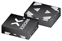 74AXP1T45GXZ1-bit dual supply translating transceiver; 3-state
Wide supply voltage range:
VCC(A): 0.9 V to 5.5 V
VCC(B): 0.9 V to 5.5 V
Low input capacitance; CI = 1.5 pF (typical)
Low output capacitance; CO = 3.8 pF (typical)
Low dynamic power consumption; CPD = 11 pF (typical)
Low static power consumption; ICC = 2 μA (25 °C maximum)
High noise immunity
Complies with JEDEC standard:
JESD8-12 (1.1 V to 1.3 V; inputs)
JESD8-11 (1.4 V to 1.6 V)
JESD8-7 (1.65 V to 1.95 V)
JESD8-5 (2.3 V to 2.7 V)
JESD8C (2.7 V to 3.6 V)
JESD12-6 (4.5 V to 5.5 V)
ESD protection:
HBM: ANSI/ESDA/JEDEC JS-001 class 2 exceeds 2000 V
CDM: ANSI/ESDA/JEDEC JS-002 class C3 exceeds 1000 V
Latch-up performance exceeds 100 mA per JESD78D Class II
Inputs accept voltages up to 5.5 V
Low noise overshoot and undershoot < 10% of VCCO
IOFF circuitry provides partial power-down mode operation
Specified from -40 °C to +125 °C
1+:¥1.0683
500+:¥0.9712
1000+:¥0.9249
3000+:¥0.8809
10000+:¥0.3668
- 10,000
- 数据手册
限量供应
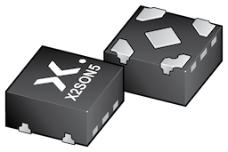
 74AUP2G32GXXLow-power dual 2-input OR gate
Wide supply voltage range from 0.8 V to 3.6 V
CMOS low power dissipation
High noise immunity
Low static power consumption; ICC = 0.9 μA (maximum)
Latch-up performance exceeds 100 mA per JESD 78 Class II Level B
Overvoltage tolerant inputs to 3.6 V
Low noise overshoot and undershoot < 10 % of VCC
IOFF circuitry provides partial Power-down mode operation
Complies with JEDEC standards:
JESD8-12 (0.8 V to 1.3 V)
JESD8-11 (0.9 V to 1.65 V)
JESD8-7 (1.2 V to 1.95 V)
JESD8-5 (1.8 V to 2.7 V)
JESD8C (2.7 V to 3.6 V)
ESD protection:
HBM: ANSI/ESDA/JEDEC JS-001 class 3A exceeds 5000 V
CDM: ANSI/ESDA/JEDEC JS-002 class C3 exceeds 1000 V
Multiple package options
Specified from -40 °C to +85 °C and -40 °C to +125 °C
1+:¥1.3734
500+:¥1.2486
1000+:¥1.1891
3000+:¥1.1325
10000+:¥0.4715
- 10,000
- 数据手册
限量供应
 74AUP2G132GXXLow-power dual 2-input NAND Schmitt trigger
Wide supply voltage range from 0.8 V to 3.6 V
CMOS low power dissipation
High noise immunity
Low static power consumption; ICC = 0.9 μA (maximum)
Latch-up performance exceeds 100 mA per JESD 78 Class II Level B
Overvoltage tolerant inputs to 3.6 V
Low noise overshoot and undershoot < 10 % of VCC
IOFF circuitry provides partial Power-down mode operation
Complies with JEDEC standards:
JESD8-12 (0.8 V to 1.3 V)
JESD8-11 (0.9 V to 1.65 V)
JESD8-7 (1.65 V to 1.95 V)
JESD8-5 (2.3 V to 2.7 V)
JESD8C (2.7 V to 3.6 V)
ESD protection:
HBM: ANSI/ESDA/JEDEC JS-001 class 3A exceeds 5000 V
CDM: ANSI/ESDA/JEDEC JS-002 class C3 exceeds 1000 V
Multiple package options
Specified from -40 °C to +85 °C and -40 °C to +125 °C
1+:¥1.3734
500+:¥1.2486
1000+:¥1.1891
3000+:¥1.1325
10000+:¥0.4715
- 10,000
- 数据手册
限量供应
 74AUP2G08GXXLow-power dual 2-input AND gate
Wide supply voltage range from 0.8 V to 3.6 V
High noise immunity
CMOS low power dissipation
Low static power consumption; ICC = 0.9 μA (maximum)
Latch-up performance exceeds 100 mA per JESD78 Class II
Overvoltage tolerant inputs to 3.6 V
Low noise overshoot and undershoot < 10 % of VCC
IOFF circuitry provides partial Power-down mode operation
Latch-up performance exceeds 100 mA per JESD 78 Class II Level B
Complies with JEDEC standards:
JESD8-12 (0.8 V to 1.3 V)
JESD8-11 (0.9 V to 1.65 V)
JESD8-7 (1.2 V to 1.95 V)
JESD8-5 (1.8 V to 2.7 V)
JESD8-B (2.7 V to 3.6 V)
ESD protection:
HBM: ANSI/ESDA/JEDEC JS-001 class 3A exceeds 5000 V
CDM: ANSI/ESDA/JEDEC JS-002 class C3 exceeds 1000 V
Multiple package options
Specified from -40 °C to +85 °C and -40 °C to +125 °C
1+:¥1.3133
500+:¥1.1939
1000+:¥1.1370
3000+:¥1.0829
10000+:¥0.4715
- 10,000
- 数据手册
限量供应
 74AUP1G38GX,125Low-power 2-input NAND gate (open drain)
Wide supply voltage range from 0.8 V to 3.6 V
CMOS low power dissipation
High noise immunity
Complies with JEDEC standards:
JESD8-12 (0.8 V to 1.3 V)
JESD8-11 (0.9 V to 1.65 V)
JESD8-7 (1.65 V to 1.95 V)
JESD8-5 (2.3 V to 2.7 V)
JESD8C (2.7 V to 3.6 V)
Low static power consumption; ICC = 0.9 μA (maximum)
Latch-up performance exceeds 100 mA per JESD 78 Class II
Overvoltage tolerant inputs to 3.6 V
Low noise overshoot and undershoot < 10 % of VCC
IOFF circuitry provides partial Power-down mode operation
ESD protection:
HBM: ANSI/ESDA/JEDEC JS-001 class 3A exceeds 5000 V
CDM: ANSI/ESDA/JEDEC JS-002 class C3 exceeds 1000 V
Multiple package options
Specified from -40 °C to +85 °C and -40 °C to +125 °C
1+:¥0.4919
500+:¥0.4472
1000+:¥0.4259
3000+:¥0.4056
10000+:¥0.3588
- 10,000
- 数据手册
限量供应
 74AUP1G132GX,125Low-power 2-input NAND Schmitt trigger
Wide supply voltage range from 0.8 V to 3.6 V
CMOS low power dissipation
High noise immunity
Overvoltage tolerant inputs to 3.6 V
Low static power consumption; ICC = 0.9 μA (maximum)
Latch-up performance exceeds 100 mA per JESD 78 Class II
Low noise overshoot and undershoot < 10 % of VCC
IOFF circuitry provides partial Power-down mode operation
Complies with JEDEC standards:
- JESD8-12 (0.8 V to 1.3 V)
- JESD8-11 (0.9 V to 1.65 V)
- JESD8-7 (1.65 V to 1.95 V)
- JESD8-5 (2.3 V to 2.7 V)
- JESD8C (2.7 V to 3.6 V )
ESD protection:
HBM: ANSI/ESDA/JEDEC JS-001 class 3A exceeds 5000 V
CDM: ANSI/ESDA/JEDEC JS-002 class C3 exceeds 1000 V
Multiple package options
Specified from -40 °C to +85 °C and -40 °C to +125 °C
1+:¥0.9265
500+:¥0.8423
1000+:¥0.8022
3000+:¥0.7640
10000+:¥0.3178
- 10,000
- 数据手册
限量供应
 74AUP1G02GX,125Low-power 2-input NOR gate
Wide supply voltage range from 0.8 V to 3.6 V
CMOS low power dissipation
High noise immunity
Overvoltage tolerant inputs to 3.6 V
Low noise overshoot and undershoot < 10 % of VCC
IOFF circuitry provides partial Power-down mode operation
Latch-up performance exceeds 100 mA per JESD 78 Class II
Low static power consumption; ICC = 0.9 μA (maximum)
Complies with JEDEC standards:
JESD8-12 (0.8 V to 1.3 V)
JESD8-11 (0.9 V to 1.65 V)
JESD8-7 (1.2 V to 1.95 V)
JESD8-5 (1.8 V to 2.7 V)
JESD8-B (2.7 V to 3.6 V)
ESD protection:
HBM: ANSI/ESDA/JEDEC JS-001 class 3A exceeds 5000 V
CDM: ANSI/ESDA/JEDEC JS-002 class C3 exceeds 1000 V
Multiple package options
Specified from -40 °C to +85 °C and -40 °C to +125 °C
1+:¥0.5061
500+:¥0.4601
1000+:¥0.4382
3000+:¥0.4173
10000+:¥0.3695
- 10,000
- 数据手册
限量供应
 74LV1T34GXHSingle supply translating buffer
Single supply voltage translator at 1.8 V, 2.5 V, 3.3 V and 5.0 V
Up translation
1.2 V to 1.8 V at VCC = 1.8 V
1.5 V to 2.5 V at VCC = 2.5 V
1.8 V to 3.3 V at VCC = 3.3 V
3.3 V to 5.0 V at VCC = 5.0 V
Down translation
3.3 V to 1.8 V at VCC = 1.8 V
3.3 V to 2.5 V at VCC = 2.5 V
5.0 V to 3.3 V at VCC = 3.3 V
5 V tolerant inputs
Latch-up performance exceeds 250 mA per JESD 78 Class II
ESD protection:
HBM: ANSI/ESDA/JEDEC JS-001 class 2 exceeds 2000 V
CDM: ANSI/ESDA/JEDEC JS-002 class C3 exceeds 1000 V
Specified from -40 °C to +85 °C and from -40 °C to +125 °C
1+:¥0.6316
500+:¥0.5742
1000+:¥0.5468
3000+:¥0.5208
9998+:¥0.3816
- 9,998
- 数据手册
限量供应
 74LVC2G00GXXDual 2-input NAND gate
Wide supply voltage range from 1.65 V to 5.5 V
5 V tolerant outputs for interfacing with 5 V logic
High noise immunity
±24 mA output drive (VCC = 3.0 V)
CMOS low power dissipation
IOFF circuitry provides partial Power-down mode operation
Complies with JEDEC standard:
JESD8-7 (1.65 V to 1.95 V)
JESD8-5 (2.3 V to 2.7 V)
JESD8-B/JESD36 (2.7 V to 3.6 V)
Latch-up performance exceeds 250 mA
Direct interface with TTL levels
Overvoltage tolerant inputs to 5.5 V
ESD protection:
HBM: ANSI/ESDA/JEDEC JS-001 class 2 exceeds 2000 V
CDM: ANSI/ESDA/JEDEC JS-002 class C3 exceeds 1000 V
Multiple package options
Specified from -40 °C to +85 °C and -40 °C to +125 °C
1+:¥1.3734
500+:¥1.2486
1000+:¥1.1891
3000+:¥1.1325
9990+:¥0.4715
- 9,990
- 数据手册
限量供应
 74LV1T00GXH2-input single supply translating NAND gate
Single supply voltage translator at 1.8 V, 2.5 V, 3.3 V and 5.0 V
Up translation
1.2 V to 1.8 V at VCC = 1.8 V
1.5 V to 2.5 V at VCC = 2.5 V
1.8 V to 3.3 V at VCC = 3.3 V
3.3 V to 5.0 V at VCC = 5.0 V
Down translation
3.3 V to 1.8 V at VCC = 1.8 V
3.3 V to 2.5 V at VCC = 2.5 V
5.0 V to 3.3 V at VCC = 3.3 V
5 V tolerant inputs
Latch-up performance exceeds 250 mA per JESD 78 Class II
ESD protection:
HBM: ANSI/ESDA/JEDEC JS-001 class 2 exceeds 2000 V
CDM: ANSI/ESDA/JEDEC JS-002 class C3 exceeds 1000 V
Specified from -40 °C to +85 °C and from -40 °C to +125 °C
1+:¥0.6316
500+:¥0.5742
1000+:¥0.5468
3000+:¥0.5208
10000+:¥0.3816
- 9,800
- 数据手册
限量供应
 74LVC1G32GX,125Single 2-input OR gate
Wide supply voltage range from 1.65 V to 5.5 V
Overvoltage tolerant inputs to 5.5 V
High noise immunity
CMOS low power dissipation
IOFF circuitry provides partial Power-down mode operation
±24 mA output drive (VCC = 3.0 V)
Latch-up performance exceeds 250 mA
Direct interface with TTL levels
Complies with JEDEC standard:
JESD8-7 (1.65 V to 1.95 V)
JESD8-5 (2.3 V to 2.7 V)
JESD8-B/JESD36 (2.7 V to 3.6 V)
ESD protection:
HBM: ANSI/ESDA/JEDEC JS-001 class 2 exceeds 2000 V
CDM: ANSI/ESDA/JEDEC JS-002 class C3 exceeds 1000 V
Multiple package options
Specified from -40 °C to +85 °C and -40 °C to +125 °C.
1+:¥0.4693
500+:¥0.4267
1000+:¥0.4064
3000+:¥0.3870
7900+:¥0.3506
- 7,900
- 数据手册
限量供应

 BUK7K32-100EX100E - Dual N-channel 100 V, 27.5 mΩ standard level MOSFET
Dual MOSFET
Q101 Compliant
Repetitive avalanche rated
Suitable for thermally demanding environments due to 175 °C rating
True standard level gate with VGS(th) rating of greater than 1 V at 175 °C
1+:¥3.6979
500+:¥3.3617
1000+:¥3.2017
3000+:¥3.0492
6000+:¥2.9386
- 6,000
- 数据手册
限量供应
 74AUP3G0434GSXLow-power dual inverter and single buffer
Wide supply voltage range from 0.8 V to 3.6 V
High noise immunity
Complies with JEDEC standards:
JESD8-12 (0.8 V to 1.3 V)
JESD8-11 (0.9 V to 1.65 V)
JESD8-7 (1.2 V to 1.95 V)
JESD8-5 (1.8 V to 2.7 V)
JESD8-B (2.7 V to 3.6 V)
Low static power consumption; ICC = 0.9 μA (maximum)
Latch-up performance exceeds 100 mA per JESD 78B Class II
Inputs accept voltages up to 3.6 V
Low noise overshoot and undershoot < 10 % of VCC
IOFF circuitry provides partial Power-down mode operation
ESD protection:
HBM: ANSI/ESDA/JEDEC JS-001 class 3A exceeds 5000 V
CDM: ANSI/ESDA/JEDEC JS-002 class C3 exceeds 1000 V
Multiple package options
Specified from -40 °C to +85 °C and -40 °C to +125 °C
1+:¥3.5439
500+:¥3.2217
1000+:¥3.0683
3000+:¥2.9222
5000+:¥1.0776
- 5,000
- 数据手册
限量供应
 74AUP2G17GM,115Low-power dual Schmitt trigger
Wide supply voltage range from 0.8 V to 3.6 V
CMOS low power dissipation
High noise immunity
Overvoltage tolerant inputs to 3.6 V
Low noise overshoot and undershoot < 10 % of VCC
IOFF circuitry provides partial power-down mode operation
Latch-up performance exceeds 100 mA per JESD 78 Class II Level B
Low static power consumption; ICC = 0.9 μA (maximum)
Complies with JEDEC standards:
JESD8-12 (0.8 V to 1.3 V)
JESD8-11 (0.9 V to 1.65 V)
JESD8-7 (1.2 V to 1.95 V)
JESD8-5 (1.8 V to 2.7 V)
JESD8C (2.7 V to 3.6 V)
ESD protection:
HBM: ANSI/ESDA/JEDEC JS-001 class 3A exceeds 5000 V
CDM: ANSI/ESDA/JEDEC JS-002 class C3 exceeds 1000 V
Multiple package options
Specified from -40 °C to +85 °C and -40 °C to +125 °C
1+:¥0.5928
500+:¥0.5389
1000+:¥0.5132
3000+:¥0.4888
5000+:¥0.4801
- 5,000
- 数据手册
限量供应
 74AUP2G126GS,115Low-power dual buffer/line driver; 3-state
Wide supply voltage range from 0.8 V to 3.6 V
High noise immunity
CMOS low power dissipation
Low static power consumption; ICC = 0.9 μA (maximum)
Latch-up performance exceeds 100 mA per JESD78 Class II
Overvoltage tolerant inputs to 3.6 V
Low noise overshoot and undershoot < 10 % of VCC
Input-disable feature allows floating input conditions
IOFF circuitry provides partial Power-down mode operation
Latch-up performance exceeds 100 mA per JESD 78 Class II Level B
Complies with JEDEC standards:
JESD8-12 (0.8 V to 1.3 V)
JESD8-11 (0.9 V to 1.65 V)
JESD8-7 (1.2 V to 1.95 V)
JESD8-5 (1.8 V to 2.7 V)
JESD8C (2.7 V to 3.6 V)
ESD protection:
HBM: ANSI/ESDA/JEDEC JS-001 class 3A exceeds 5000 V
CDM: ANSI/ESDA/JEDEC JS-002 class C3 exceeds 1000 V
Multiple package options
Specified from -40 °C to +85 °C and -40 °C to +125 °C
1+:¥0.8612
500+:¥0.7829
1000+:¥0.7456
3000+:¥0.7101
5000+:¥0.6284
- 5,000
- 数据手册
限量供应